- 您现在的位置:买卖IC网 > Sheet目录481 > MTP50P03HDL (ON Semiconductor)MOSFET P-CH 30V 50A TO-220AB
�� �
�
�MTP50P03HDL�
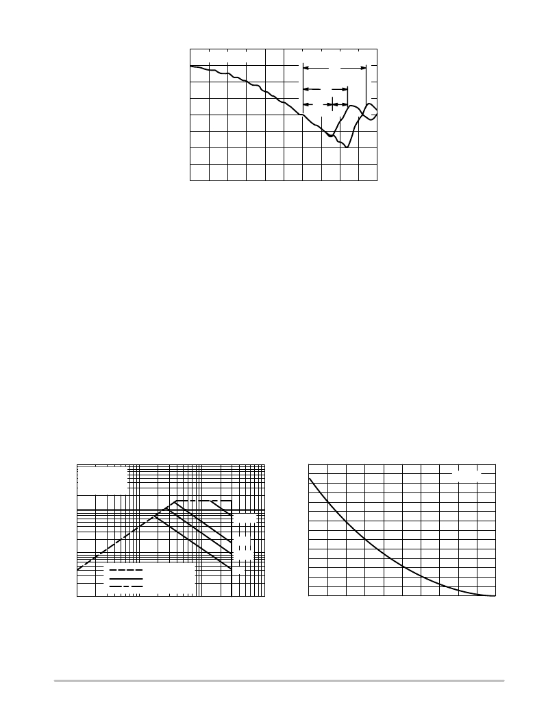
�di/dt = 300 A/� m� s�
�Standard� Cell� Density�
�t� rr�
�High� Cell� Density�
�t� a�
�t� rr�
�t� b�
�t,� TIME�
�Figure� 11.� Reverse� Recovery� Time� (t� rr� )�
�SAFE� OPERATING� AREA�
�The� Forward� Biased� Safe� Operating� Area� curves� define�
�the� maximum� simultaneous� drain?to?source� voltage� and�
�drain� current� that� a� transistor� can� handle� safely� when� it� is�
�forward� biased.� Curves� are� based� upon� maximum� peak�
�junction� temperature� and� a� case� temperature� (T� C� )� of� 25� °� C.�
�Peak� repetitive� pulsed� power� limits� are� determined� by� using�
�the� thermal� response� data� in� conjunction� with� the� procedures�
�discussed� in� AN569,� “Transient� Thermal� Resistance� ?�
�General� Data� and� Its� Use.”�
�Switching� between� the� off?state� and� the� on?state� may�
�traverse� any� load� line� provided� neither� rated� peak� current�
�(I� DM� )� nor� rated� voltage� (V� DSS� )� is� exceeded,� and� that� the�
�transition� time� (t� r� ,� t� f� )� does� not� exceed� 10� m� s.� In� addition� the�
�total� power� averaged� over� a� complete� switching� cycle� must�
�not� exceed� (T� J(MAX)� ?� T� C� )/(R� q� JC� ).�
�A� power� MOSFET� designated� E?FET� can� be� safely� used�
�in� switching� circuits� with� unclamped� inductive� loads.� For�
�1000�
�reliable� operation,� the� stored� energy� from� circuit� inductance�
�dissipated� in� the� transistor� while� in� avalanche� must� be� less�
�than� the� rated� limit� and� must� be� adjusted� for� operating�
�conditions� differing� from� those� specified.� Although� industry�
�practice� is� to� rate� in� terms� of� energy,� avalanche� energy�
�capability� is� not� a� constant.� The� energy� rating� decreases�
�non?linearly� with� an� increase� of� peak� current� in� avalanche�
�and� peak� junction� temperature.�
�Although� many� E?FETs� can� withstand� the� stress� of�
�drain?to?source� avalanche� at� currents� up� to� rated� pulsed�
�current� (I� DM� ),� the� energy� rating� is� specified� at� rated�
�continuous� current� (I� D� ),� in� accordance� with� industry�
�custom.� The� energy� rating� must� be� derated� for� temperature�
�as� shown� in� the� accompanying� graph� (Figure� 13).� Maximum�
�energy� at� currents� below� rated� continuous� I� D� can� safely� be�
�assumed� to� equal� the� values� indicated.�
�1400�
�100�
�V� GS� =� 20� V�
�SINGLE� PULSE�
�T� C� =� 25� °� C�
�100� m� s�
�1� ms�
�1200�
�1000�
�800�
�600�
�I� D� = 50 A�
�10�
�10 ms�
�400�
�R� DS(on)� LIMIT�
�THERMAL� LIMIT�
�PACKAGE� LIMIT�
�dc�
�200�
�1�
�0.1�
�1.0�
�10�
�100�
�0�
�25�
�50�
�75�
�100�
�125�
�150�
�V� DS� ,� DRAIN?TO?SOURCE� VOLTAGE� (VOLTS)�
�Figure� 12.� Maximum� Rated� Forward� Biased�
�Safe� Operating� Area�
�T� J� ,� STARTING� JUNCTION� TEMPERATURE� (� °� C)�
�Figure� 13.� Maximum� Avalanche� Energy� versus�
�Starting� Junction� Temperature�
�http://onsemi.com�
�6�
�发布紧急采购,3分钟左右您将得到回复。
相关PDF资料
MTPD1346-010
PIN DIODE 1300NM FLAT 2.8MM TO46
MTPD1346-030
PIN DIODE 1300NM FLAT 2.8MM TO46
MTPD1346-100
PIN DIODE 1300NM FLAT 2.8MM TO46
MTPS1065PT
VISIBLE RED POINT SOURCE EMITTER
MTPS1065WC
VISIBLE RED POINT SOURCE EMITTER
MTPS3085CP
EMITTER IR POINT SOURCE
MTPS3085MC
EMITTER IR POINT SOURCE
MTPS3085MT
EMITTER IR POINT SOURCE
相关代理商/技术参数
MTP50P03HDLG
功能描述:MOSFET PFET T0220 30V 50A 25mOhm RoHS:否 制造商:STMicroelectronics 晶体管极性:N-Channel 汲极/源极击穿电压:650 V 闸/源击穿电压:25 V 漏极连续电流:130 A 电阻汲极/源极 RDS(导通):0.014 Ohms 配置:Single 最大工作温度: 安装风格:Through Hole 封装 / 箱体:Max247 封装:Tube
MTP50P03HDLG
制造商:ON Semiconductor 功能描述:MOSFET P TO-220
MTP50S
制造商:NELLSEMI 制造商全称:Nell Semiconductor Co., Ltd 功能描述:Three-Phase Bridge Rectifier, 50A
MTP50W
制造商:NELLSEMI 制造商全称:Nell Semiconductor Co., Ltd 功能描述:Glass Passivated Triple-Phase Bridge Rectifier, 50A
MTP5210F3
制造商:CYSTEKEC 制造商全称:Cystech Electonics Corp. 功能描述:P-Channel Enhancement Mode Power MOSFET
MTP52K3BPNO
功能描述:插线板 3 1/2 UNWIRED IDC B
RoHS:否 制造商:Switchcraft 产品类型:Bantam (TT) 正规化: 高度/机架数量: 深度: 端接类型: 位置/触点数量:48
MTP52K3BPNOX
功能描述:CONN JACK 48 MTP BACKPANEL 3.5" RoHS:是 类别:盒,外壳,支架 >> 插线台,插座面板 系列:MTPBP 标准包装:1 系列:TT96 类型:音频插孔面板 连接器类型:0.173" 耳机插孔 位置数:96 行数:2 端接类型:焊接
MTP52N06V
制造商:MOTOROLA 制造商全称:Motorola, Inc 功能描述:TMOS POWER FET 52 AMPERES 60 VOLTS RDS(on) = 0.022 OHM